Laboratory 4 - Prototyping Laboratory.
The Prototyping Laboratory is a facility which aims at developing new research directions in the field of eco-nano-technologies and advanced materials, but also in innovative devices on large surfaces, up to 200 mm, in the fields of electronics and optoelectronics, sensors, energy production and storage:
- Surface processing and nanostructuring services with FiB / SEM equipment;
- Development of FET type devices for measuring the opto-electrical characteristics of nanomaterials on surfaces up to 200 mm2;
- Development of MEMS, Optical MEMS devices;
- Development of sensor devices or sensor arrays on surfaces up to 200 mm2.
|
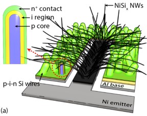
Connecting wire-based solar cells without any transparent conducting electrode Le To Toan et al CrystEngComm, 2016 |
The activity of the prototyping laboratory falls within the directions 2 and 3 of the themes of the INFLPR strategy;
Dir. 2 - Sensor platforms based on photonic and plasma methods
-
Optoacoustic systems for real-time gas detection,
-
Fiber-optic sensors for gas detection,
-
Methods of detection based on Raman scattering of relevant pharmaceutical compounds,
-
Surface acoustic wave sensors for the detection of volatile organic compounds and UV radiation,
-
Chemoresistive sensors based on thin films deposited by laser techniques.
Dir. 3 - Nanostructures and advanced materials obtained / characterized by laser, plasma and radiation methods for eco-nano-technologies
-
Advanced and highly nanostructured materials obtained by plasma and laser methods,
-
Photonic processing of new materials for eco-nano-technologies,
-
Special crystals and ceramics for laser sources and advanced radiation conversion processes.
Institutional equipment / facilities;
-
Photolithography system
-
Nanolithography system
-
Encapsulation system (coating / development)
-
FIB-SEM ion-focused beam scanning electron microscope
-
Sensor testing system under controlled conditions
Equipment specifications
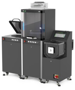
- Complete IDONUS Photolithography System including mask alignment system and AMCOSS coating / development system
|
Mask alignment system |
|
Coverage / development system |
responsible staff - Mihai Zamfir, Mihai Darlau (AMCOSS)
users - MIhai Sopronyi
-
Thermo Fisher Scientific Verios nanolithography system
responsible staff - Mihai Zamfir, Mihai Darlau (AMCOSS)
users - MIhai Sopronyi
-
Thermo Fisher Scientific Scios Dual Beam FiB-SEM with Ga/Pt patterning capabilities
responsible staff - Mihai Zamfir, Mihai Darlau (AMCOSS)
users - Anca Bonciu, Isabela Bancu, Ioan Ghitiu
-
Sensor testing system under controlled conditions
responsible staff - Mihai Zamfir
users -
Laboratory Team
 Responsible of Laboratory
Dr. Mihai-Robert Zamfir

Dr. Anca Bonciu
Dr. Mihai Sopronyi

Tech. Mihai Darlau
Research and development activity:
-
Development of innovative energy storage and production systems and devices based on emerging and alternative technologies,
-
Fundamental research of two-dimensional (2D) materials with innovative physical and chemical properties and exploring the possibilities of integrating them into devices with different architectures for applications in various fields,
-
Development of complex optoelectronic heterostructures,
-
Development of “MEMS”, “Optical MEMS” type devices, etc.,
-
Development of functional devices for bionanophotonics: micro-nano-fluidics, sensors.