Laboratory 2 - Analysis, Characterization, Testing.
The mission of the "Analysis, Characterization, Testing" laboratory is to characterize the properties of materials processed by laser, plasma and radiation, of devices obtained in the laboratories of the institute and provide testing and characterization services to businesses or institutions (universities / research institutes) that do not have high-performance testing capabilities.
Services offered:
- Structural and mechanical analysis center for materials subjected to thermal / mechanical stress;
- Electron microscopy center;
 Morphological-structural characterization of thin films over large areas and of materials processed with laser beams, plasma and radiation;
- Characterization of electrical, magnetic and optical properties of materials processed with laser, plasma and radiation;
- Mechanical characterization services for thin films used in hostile environments (high temperatures, humidity).
|
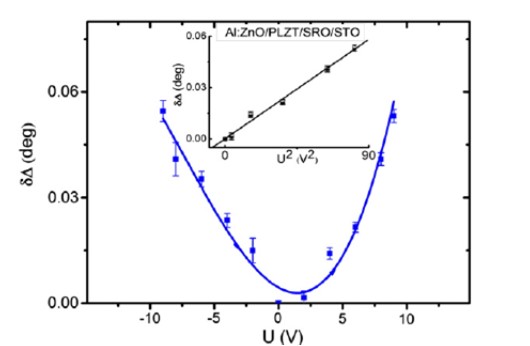
Electro-optic and dielectric properties of epitaxial Pb1 - 3x / 2LaxZr0.2Ti0.8O3 thin films obtained by pulsed laser deposition, N.D.Scarisoreanu et al, Thin Solid Films (2013) |
Institutional equipment / facilities;
-
 Cryostatic system for testing electrical, transport and magnetic properties
 -
Test system for mechanical properties at high temperatures and in humid conditions (Tribonanoidentor)
-
Large area solar simulator and photovoltaic quantum spectral efficiency test system
-
Surface energy / wettability measuring equipment (Static and dynamic contact angle microscope)
-
Spectro-elipsometer
-
High Resolution Transmission Electron Microscope (HR TEM)
-
TEM sample preparation equipment
-
BET porosimeter
-
DLS nanometer particle size analyzer
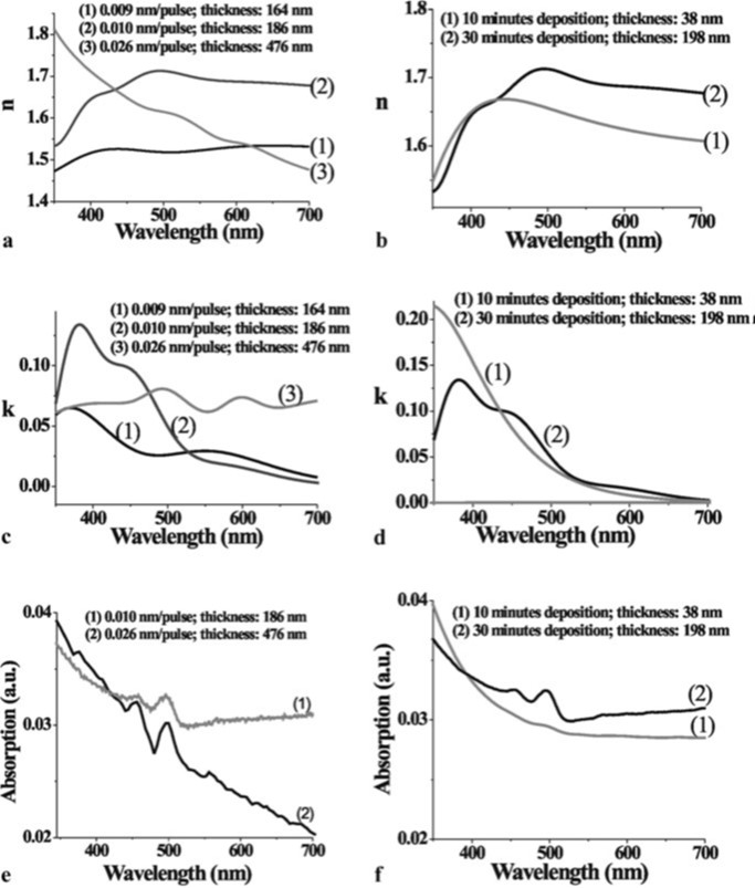
| MAPLE deposition of PEG: PLGA thin films, Irina Alexandra Paun et al, Appl Phys A (2012) |
Equipment specifications

-
High resolution TEM and STEM microscope for all materials science and semiconductor applications:
The High Resolution Spectra 300 S/TEM microscope provides unique material characterization capabilities thanks to it's state of the art configuration:
- Monochromated 300kV X-FEG source
- Probe corrector
- High solid angle EDS detector (more than 2.2)
- EMPAD detector for 4DSTEM analysis
responsible staff - Nicu Scarisoreanu - C400.
users - Valentin Ion, Nicu Scarisoreanu, Anca Bonciu, Ioan Ghitiu
- TEM test preparation equipment
- Gatan Ultrasonic Cutter - Ultrasonic cutting machine
- TEM Gatan Dimple Grinder 1 - Sample polishing machine
- TEM Gatan Disc Grinder - Polishing machine for pre-thin samples
- Specimen Punch - Gatan Disk Punch - System for cutting metal specimens with a diameter of 3mm
- Plasma Cleaner - Fischione Plasma Cleaner 1020 - TEM sample decontamination machine with plasma
- Ion Milling - Gatan PIPS II 695 Pro - Ion TEM sample grinding/drilling machine
- Buehler IsoMet 1000 - System for initial cutting of samples with diamond disc
responsible staff - Valentin Ion - C400.
users - Valentin Ion, Cristian Borz, Ioan Ghitiu
-
Cryostatic system for testing electrical, transport and magnetic properties
Testing electrical and magnetic properties for thin layers and nanostructures:
- I-V, C-V, electrical resistivity
- magnetoresistivity over a wide temperature range (4.2 K - 725 K)
responsible staff - Mihai Zamfir - C400
users - Valentin Ion, Isabela Bancu, Ioan Ghitiu, Andrei Stoichioiu - S200.
-
Mechanical properties testing system at high temperatures and in humid conditions
(Tribonanoidentor);
- Identification range: 100 μm
- Load range: 50 mN or 100 mN max
- Resolution: 0.003 nm
- Depth noise floor: 0.03 nm
- Load resolution: 3 nN
- Load noise floor: ~ 0.1 mN
- Reference with own piezo actuator and load sensor
- Drift ~ 1ppm / ° C
responsible staff - Urzica Iuliana - S200, Bonciu Anca Florina - C400.
users - Baiasu Flaviu Florin, Porosnicu Corneliu, Manica Dumitru, Bonciu Anca Florina, Ivan Raluca Mihaela, Urzica Iuliana, Craciun Valentin, Duta Liviu Marian.
-
Large area solar simulator and photovoltaic quantum spectral efficiency test system
- Monochromator with 300 mm focal length
- Variable range 350 - 1800 nm
- Condensing and focusing optics
- Collimated area 110 x 110 mm
- Spectral and temporal class A
responsible staff - Andrei Florin - C400, Stoichioiu Andrei - S200.
users - Mihailescu Andreea, Stoichioiu Andrei, Bita Bogdan, Garoi Petronela, Viespe Cristian, Andrei Florin, Manica Dumitru.
-
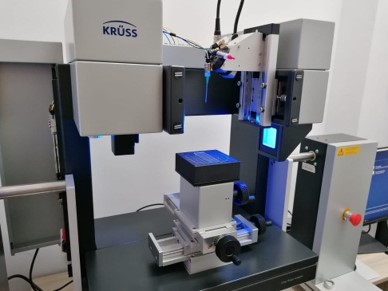 Surface energy / wettability measuring equipment (Static and dynamic contact angle microscope);
- Automated system for contact angle determination (in the range of 1-180 degrees, resolution 0.1 degrees) and surface energy
- Automatic dosing system with at least 3 liquids, drop resolution of 0.1 microliters and manual dosing
- Temperature controlled room (30 - 160 ° C)
- Humidity control system (15 - 85%)
- Possibility of tilting to determine the dynamic angle
responsible staff - Mitu Bogdana - C400
users - Mitu Bogdana
-
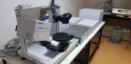 Spectro-ellipsometer
- Spectral range 190 - 2100 nm
- Temperature range 190 - 350 °C
- Measured area 200 x 200 mm
- Scan time across the entire spectrum of 15 min
- Variable diameter of the incident spot 80 microns -1 mm
responsible staff - Ion Valentin - C400
users - Ion Valentin
-
BET porosimeter
- Pressure transducer system for various fields with automatic change
- Thermal correction, adjustable according to the adsorbent and cell geometry
- Pore volume (liquid): sensitivity: 10-9 ml / g
- Adsorbed volume (STP): sensitivity: 5 x 10⁻⁸ cc / g
- Pore size: diameters between 3.5….> 5000 Å
responsible staff - Fleaca Claudiu - S200
users - Ion Morjan, Chiolbasu Diana, Fleaca Claudiu, Porosnicu Ioana, Zarif Maria, Dumitrache Florian.
-
DLS nanometer particle size analyzer
- Particle size analysis range: 0.4 - 10000 nm particle diameter
- Size distribution 0. 2 - 15,000 nm
responsible staff - Dumitrache Florian - S200
users - Dumitrache Florian, Ardelean Alina, Axente Emanuel, Badea Florin, Antohe Iulia, Dinache Andra.
-
Interferometer (Analysis of optical surfaces with diameter larger than 100 mm)
responsible staff - Andrei Florin - C400
users - Stanciu George, Broasca Alin, Andrei Florin, Urzica Iuliana.
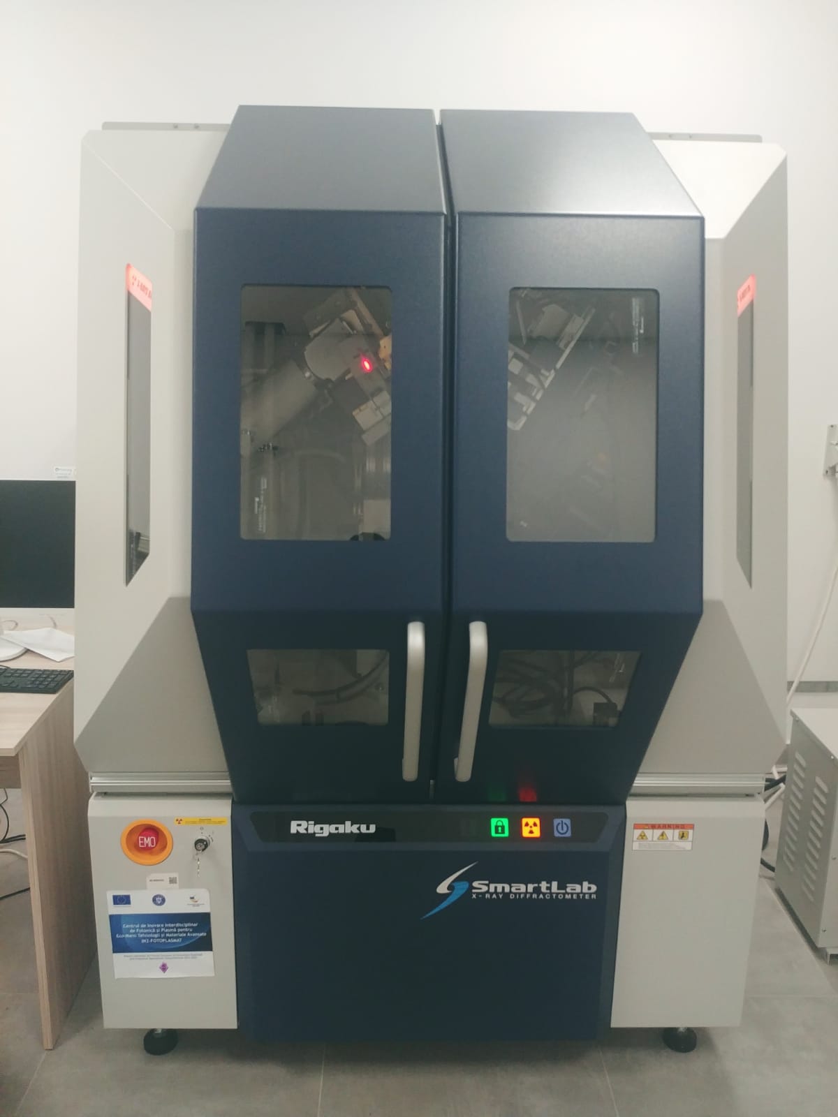
- X-Ray Diffractometer: Rigaku SmartLab
- Automated high-resolution θ-θ multipurpose X-ray diffractometer (XRD)
- Powerful 3kW X-Ray source
- CBO optics
- D/Tex Ultra 250 detector
- Powder and thin film diffraction, SAXS, in-plane scattering.
Laboratory Team
Acting Head of Laboratory
Dr. Valentin Ion - CS2
Drd. Luiza Maria Stingescu - ACS
Drd. Elena-Isabela Bancu - ACS
Drd. Ioan Mihail Ghitiu - ACS
Perspectives - Research and development activity:
-
Structural analysis activities by high-resolution transmission electron microscopy and X-ray diffraction of ceramic materials, nanostructures, large-area thin layers of advanced oxide, oxynitric and metallic materials for operation in extreme conditions;
-
Characterization of optical, electrical and magnetic properties over a wide temperature range;
-
Optical characterizations of thin films deposited on large areas by PLD; Mapping of the optical properties and thicknesses of the deposited thin films on areas up to 200 x 200 mm;
-
Highlighting phase transformations in the case of ferroelectric and / or multiferoic films;
-
Characterization of the tribological properties of the thin films obtained by laser and plasma deposition techniques;
-
Measurements of contact angle, surface tension of liquids and the surface free energy of solids.